My research focuses on semiconductor device physics and advanced integration approaches, spanning carbon nanotube field emission devices, photonic packaging, and epitaxial graphene. I’ve fabricated some pretty cool devices as well as built equipment to fabricate and test them. Below are a few if my research projects during my undergraduate career. Always looking to learn more in the realm of semiconductor devices/fabrication!
Carbon Nanotube Field Emissions Cathodes (CNTFEC)
Overview
Fabrication & Methods
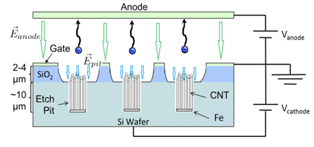
Cathodes are a fundamental component in electron emission devices, serving as the source of electrons for applications such as hall effect thrusters and electron microscopy.
Field emission cathodes (FECs) offer a compelling alternative to thermionic cathodes by leveraging quantum tunneling to extract electrons utilizing electric fields to narrow the potential barrier.
The localized electric field is dependent the field enhancement factor ꞵ; carbon nanotubes (CNTs) maximize the ꞵ due to their high aspect ratio geometry, significantly lowering the threshold electric field necessary for tunneling.
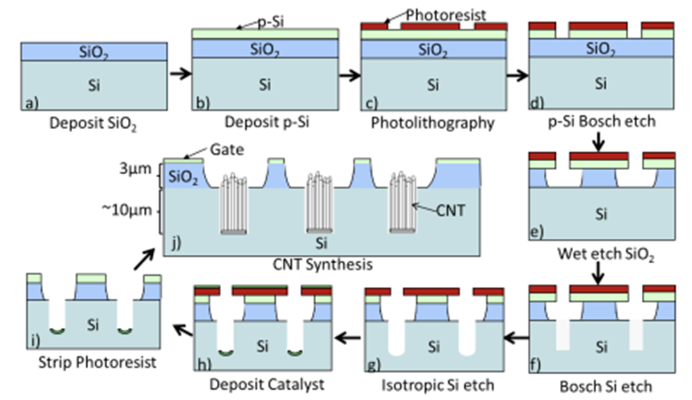
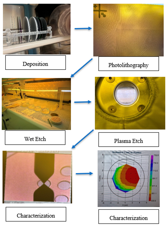
The fabrication of CNTFECs integrates both conventional semiconductor processing and nanomaterial synthesis. Starting at the wafer scale, layers of silicon dioxide and polysilicon are deposited through LPCVD, patterned through photolithography, and etched using a combination of wet and plasma etching steps to define gate, trench, and contact structures.
Subsequent Bosch etching and isotropic silicon etching refine pit geometry with high aspect ratio.
The fabrication process begins with wafer preparation. N-type, phosphorus-doped silicon wafers are used to ensure conductivity and electron availability.
A standard CMOS cleaning sequence (SC1, SC2, Piranha etch for organics, and a light HF dip for native oxide removal) is applied. A 3.2 µm thermal oxide is then grown in a tube furnace to serve as the insulating layer, followed by deposition of polysilicon, which is degenerately doped with phosphorus to function as the gate electrode.
Using photolithography with 4 µm pit masks at varied spacings, up to 64 chips can be patterned per 4-inch wafer.
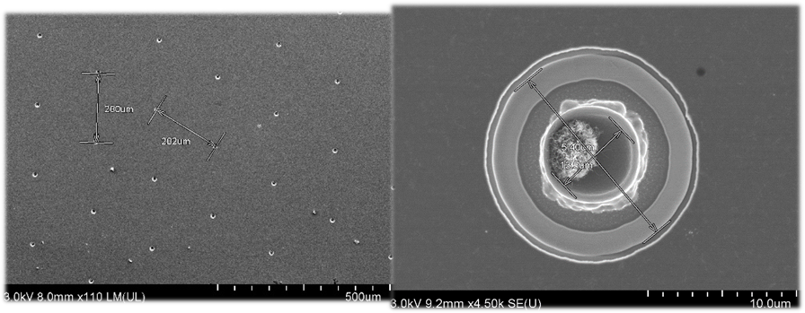
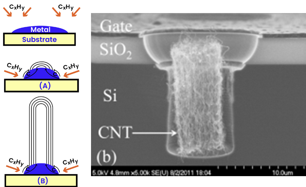
Pit formation proved to be the most challenging stage, requiring careful process development and metrology to define features reliably. Success depended on optimized DRIE of polysilicon, BOE etching of oxide, and Bosch silicon etching.
Frequent issues ranging from equipment faults, process variability, and photomask alignment required close collaboration with cleanroom process staff to troubleshoot and refine recipes.
Once pits were successfully defined, a catalyst stack was deposited by line-of-sight PVD. Lift-off ensured the catalyst remined only at the pit bottoms, enabling localized CNT growth.
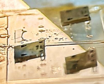
After completing wafer-level fabrication, the wafers were diced into individual chips, packaged, and prepared for electrical testing.
Results & Applications
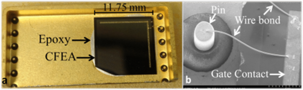
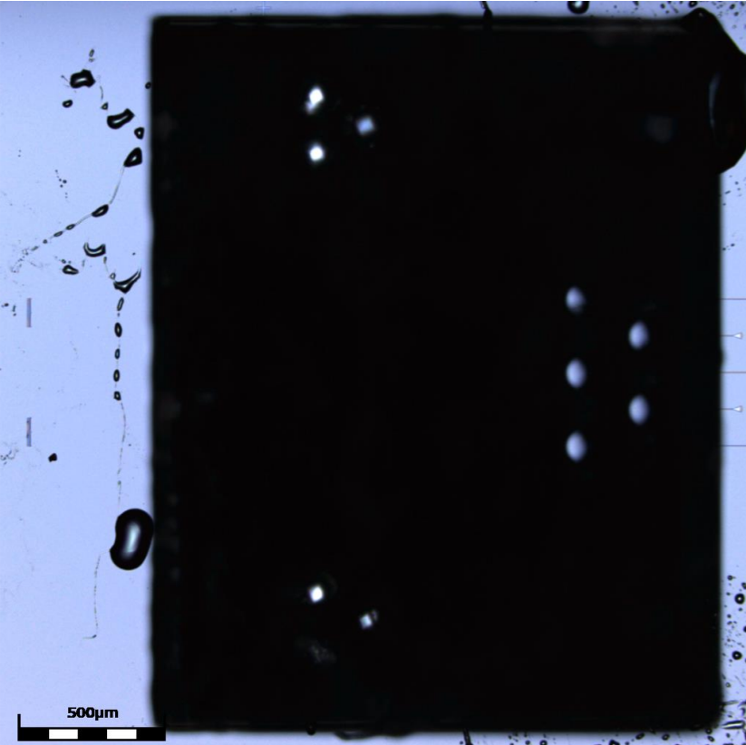
After individual chips are made, they are silver epoxied onto a gold package and wire bonded for electrical emissions testing. The gate layer is kept at ground, while the negative bias in the substrate is varied.
On going research is being done to refine the fabrication methods for higher yield as well as optimize performance.
I’ve simulated emissions results in COMSOL multiphysics to find optimal parameters, and current work involves maximizing current emission for CNTFECs.
Current best chip field emissions are at ~290 µA/cm2 at 250V negative bias on the substrate with a CNTFEC active area of 0.347 cm2
By optimizing pit geometries and refining growth of CNTFECs, up to 10x current emissions can be produced per chip!
G. Feng, J. Ready, “Optimizing Carbon Nanotube Field Emission Cathodes: Height-Dependent Performance and Emission Enhancement,” TMS 2024 Annual Meeting & Exhibition, Las Vegas, NV, March 3–7, 2024. Poster presentation.
Photonic Packaging
Overview
Photonic packaging is essential for scaling silicon photonics in high-bandwidth systems. Our work introduces Fiber-Interconnect Silicon Chiplet Technology with Tilt (FISCT-T), which achieves passive, tilt-controlled fiber alignment using through-silicon holes, bonded microspheres, and lithographically defined self-aligned structures. This approach eliminates active alignment, enabling low-loss, scalable fiber-to-chip coupling for next-generation photonic integration.
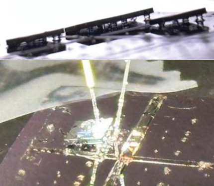
Fabrication & Methods
The FISCT-T platform consists of two co-designed components: a silicon photonic integrated circuit (PIC) with lithographically defined Positive Self-Aligned Structures (PSAS), and a tilted-silicon chiplet (TSC) containing through-silicon holes (TSHs) for fiber and microsphere placement.
On the PIC, PSAS features are patterned in thick photoresist, thermally reflowed to form smooth dome and ring geometries, and aligned to underlying grating couplers. On the chiplet side, TSHs are etched by Bosch DRIE to create precision sites for fibers and microspheres. Monodisperse microspheres are bonded into the chiplet holes with UV-curable adhesive, after which the chiplet is flipped and bonded to the PIC. During assembly, the microspheres engage the PSAS features to define a fixed tilt (~9°) and sub-micron lateral positioning, eliminating the need for active alignment.
This co-design of photonic and mechanical structures enables wafer-scale fabrication of thousands of chiplets per wafer, with high reproducibility and robustness for passive photonic packaging.
Results & Applications
The FISCT-T platform enables low-loss, scalable fiber coupling for silicon photonics, making it well-suited for co-packaged optics, wafer-level testing, and high-density photonic integration in data centers, AI accelerators, and advanced communication systems. Its passive alignment approach reduces packaging cost and complexity, while supporting heterogeneous integration across diverse PIC platforms.
Epitaxial Graphene
Overview
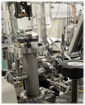
I worked in the Epigraphene Lab at Georgia Tech, focusing on the growth and characterization of epitaxial graphene on SiC for high-mobility electronic applications. I performed Raman spectroscopy, ellipsometry, AFM, and Van der Pauw probing to assess material and device properties, and I also designed and built custom PVD and characterization equipment to support graphene processing and evaluation.
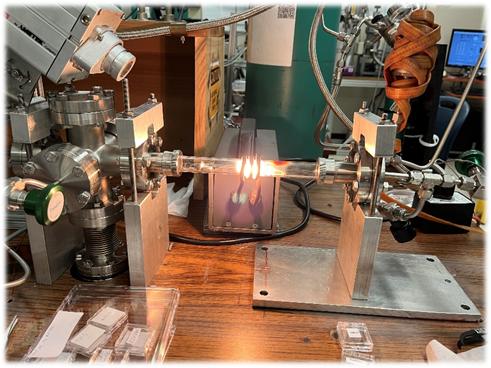
Tube furnace where Si is evaporated off the SiC carbon interface to create a monolayer of graphene
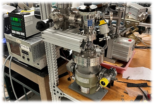
PVD selenium furnace I designed and put together using spare HV parts. Includes crystal sensor for monitoring deposition rate and current thickness; calibrated through confirmation on AFM scratch test. Selenium is used to shield graphene from the atmosphere.
Heat tape heats the crucible section to around 300 degrees celcius, evaporating it onto the sample at the top of the chamber, controlled by a manual shutter
Carbon evaporator for SEM measurements I reassembled
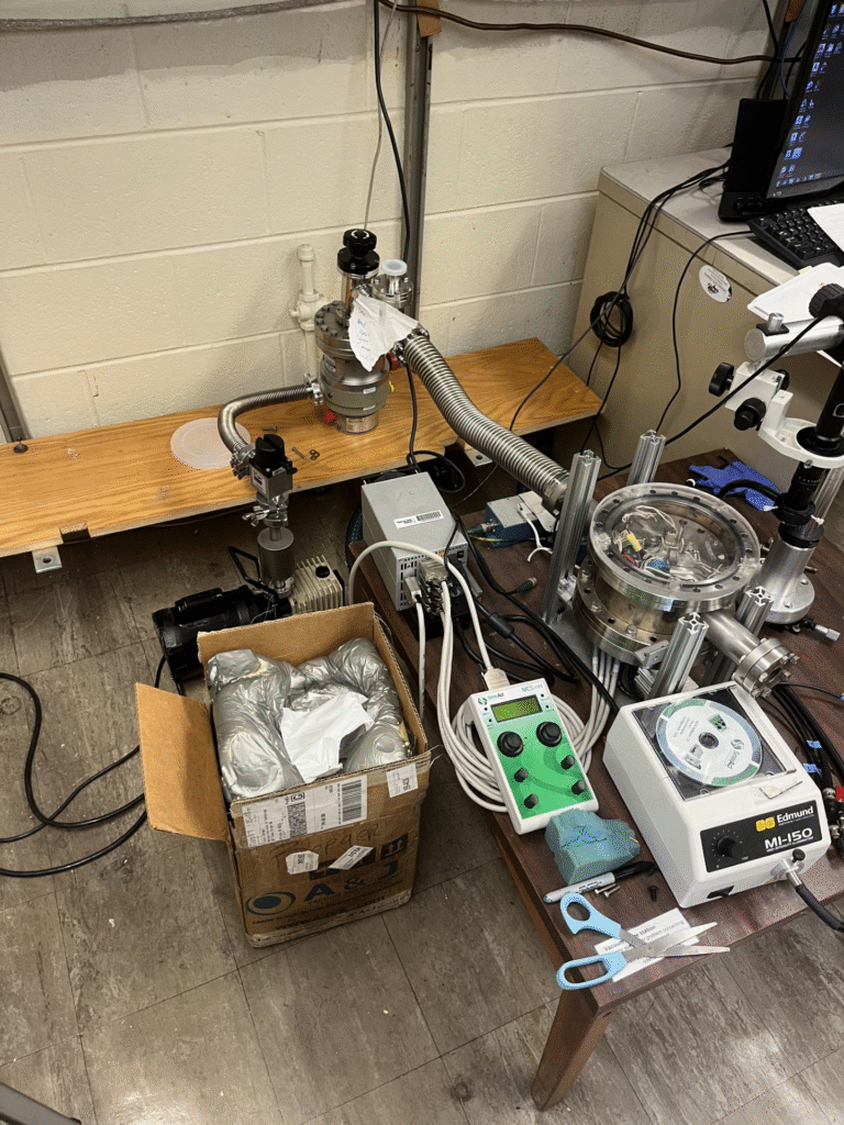
Vacuum Probe station I assembled for characterizing graphene at various pressures and gas doping variations