EECS PhD student · MIT

Gabriel Feng

Semiconductor devices: physics, fabrication, packaging.

→ next   F full screen

About me

Devices, from the physics to the fab

Education

  • MIT · EECS PhD, Stata Presidential Fellow
  • Georgia Tech · B.S. Physics, B.S. EE

Research

  • GaN HEMTs
  • 2D materials
  • CNT field emitters
  • Photonic packaging
  • Epitaxial graphene

Industry

  • Northrop Grumman
  • Samsung Semiconductor
  • IBM Research
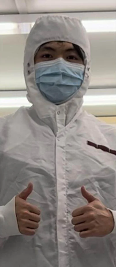
Gabriel in a cleanroom suit, giving two thumbs up

Georgia Tech · CNT field emitters · 1 / 3

Cold cathodes from carbon nanotubes

  • Field emission, no hot filament
  • CNT aspect ratio → high β
  • Integrated gate → low-voltage control

J ∝ Eloc2 exp(−b φ3/2 / Eloc),   Eloc = β E

GTRI · President’s Undergraduate Research Award
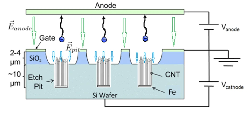
Schematic of a gated carbon-nanotube field emitter: CNTs in etched pits under a gate, with an anode above
Gated CNT emitter
energydistance from the tip CNT tip Fermi level no field with field βE φ tunnels through

Georgia Tech · CNT field emitters · 2 / 3

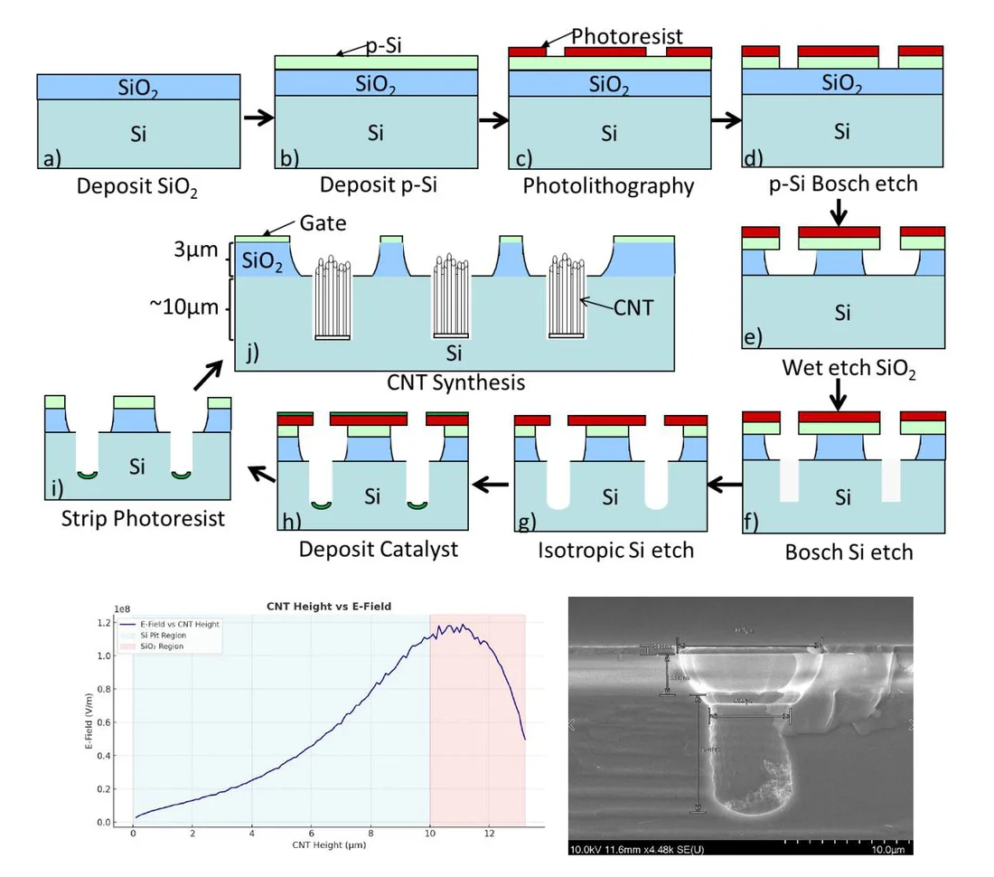
Designed, simulated, then built

  • COMSOL field + TCAD process models
  • Oxide → poly-Si gate → litho → Bosch etch → CNT growth
  • SEM-EDS root-caused failed chips
  • 10+ refinements → one-weekend run
The CNT emitter process flow from oxide deposition to CNT synthesis, a plot of field against CNT height, and an SEM cross-section of a failed sample
Process flow · tip field vs CNT height · failure SEM

Georgia Tech · CNT field emitters · 3 / 3

Repeatable gated emission

~240 mA/cm²
CNT growth area
~300 µA/cm²
whole device
~14×
a recent self-charging-gate cathode*
  • Fowler–Nordheim, matches simulation
  • Next: stability, SiNx gate

TMS 2024, 2025 · *Xiao et al., Nat. Commun. 15, 764 (2024)
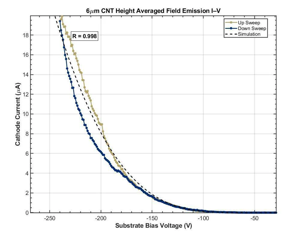
Cathode current against substrate bias, up and down sweeps averaged over 50 cycles, with the simulation
I–V, 50 cycles, with simulation
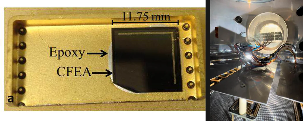
A CNT emitter chip epoxied into a package, and the vacuum emission test setup
Packaged chip · vacuum setup

Georgia Tech

Also at Georgia Tech

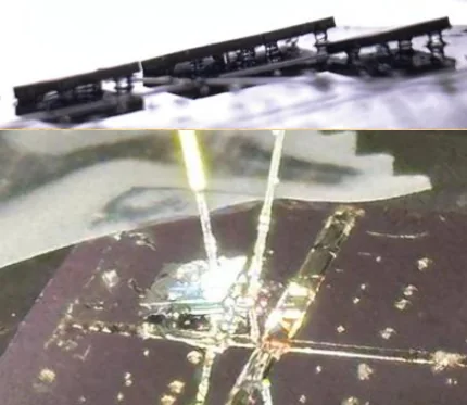
Tilted silicon chiplet with optical fibers inserted

Photonic packaging: FISCT-T

Passive fiber alignment: ~9° tilt, sub-µm placement

Yu, Feng, Gaylord, Bakir · IEEE PTL (under revision)
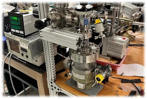
High-vacuum PVD selenium furnace

Epitaxial graphene on SiC

~1700 °C growth on SiC · built the furnace, evaporator, probe station

Industry · 2024 · Northrop Grumman

Dielectric films for RF devices

Process Engineering Intern · Advanced Technology Lab

  • ALD / CVD films in spec, with SPC
  • Zero-stress ALD Al2O3
  • Si3N4 contact angle −80%
  • Precursor model recovered a wafer lot
Film stress, ALD Al₂O₃ compressivenet zerotensile plasma + thermal mix Contact angle, PECVD Si₃N₄ beforeafter: angle ~80% lower

Industry · 2025 · Samsung Austin Semiconductor

Finding the defects that matter

Metrology Applications Intern

  • 14 nm FinFET critical defects
  • Recipe-scoring app + CNN detector
  • Up to 117% better detection
  • 4 nm polarization studies · FMEA

Live: my WM-811K CNN, 90.1% on held-out wafers · data: Wu et al., IEEE TSM 28, 1 (2015)

Public WM-811K data · live

Industry · 2026 · IBM Research

Co-packaged optics, device to EDA

R&D Intern · Albany, NY · Dr. Will Green

  • Mono-taper: −44% footprint, taped out
  • 3D photonic routing: A* + congestion
  • TCAD migration agent
Adiabatic mono-taper conventional taper mono-taper44% smaller Photonic routing: A* + negotiated congestion

MIT · GaN HEMT

A baseline GaN HEMT at MIT.nano

18 tools
qualified, first month
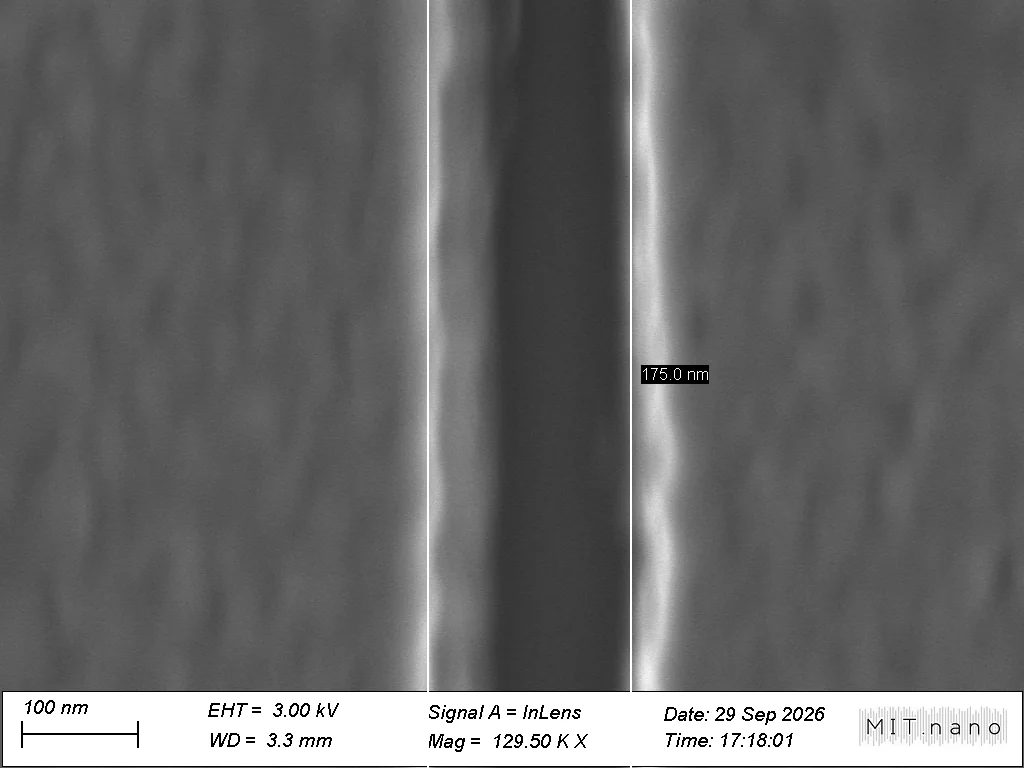
~170 nm
source–drain gap
0.66–0.72
Ω·mm contacts, 4 / 4 samples
  • Next: gate → LSD 100–600 nm, Au-free
SEM of the source-drain gap of the most scaled device, about 170 nanometres wide
SEM · ~170 nm gap
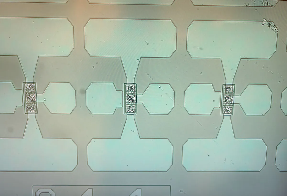
Optical micrograph of three HEMTs with ohmic contacts on mesas and their pads
After ohmics, mesa, pads

MIT · GaN HEMT · process

Calibrating every step

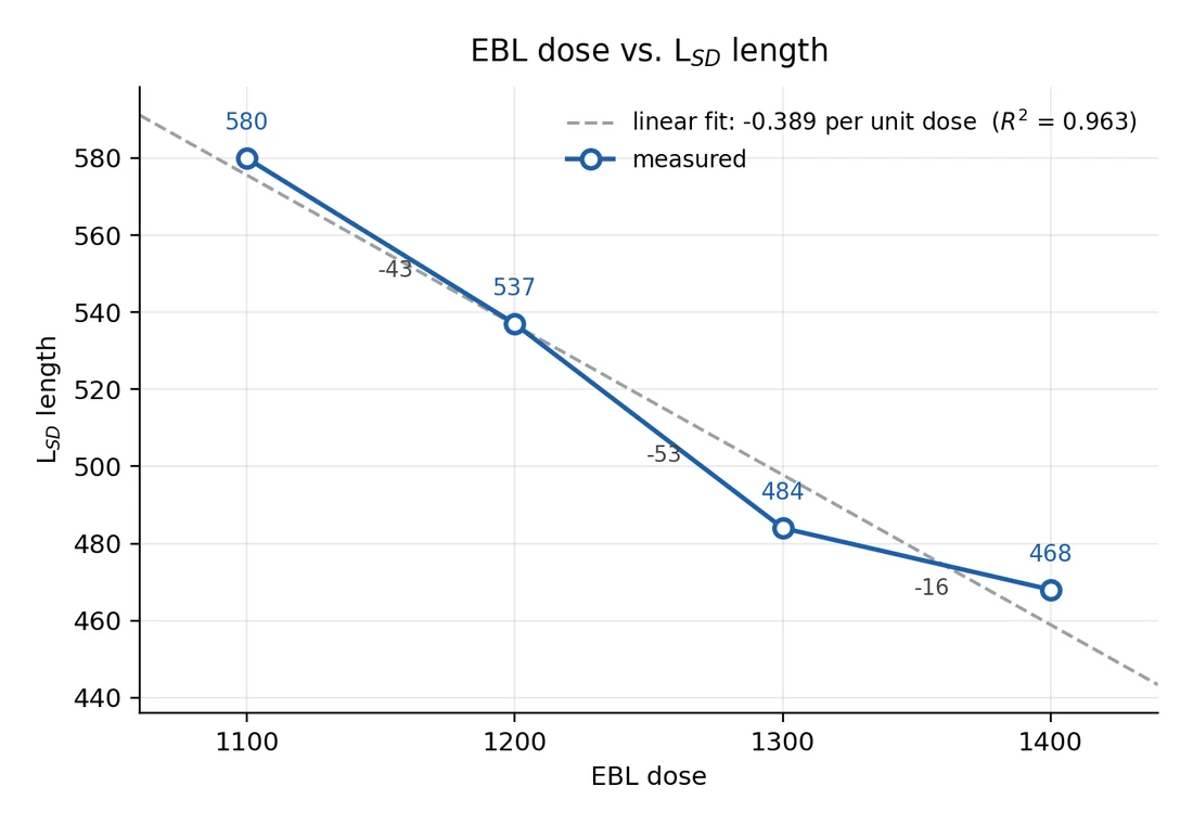
  • Dose · −0.39 nm per µC/cm², R² 0.96
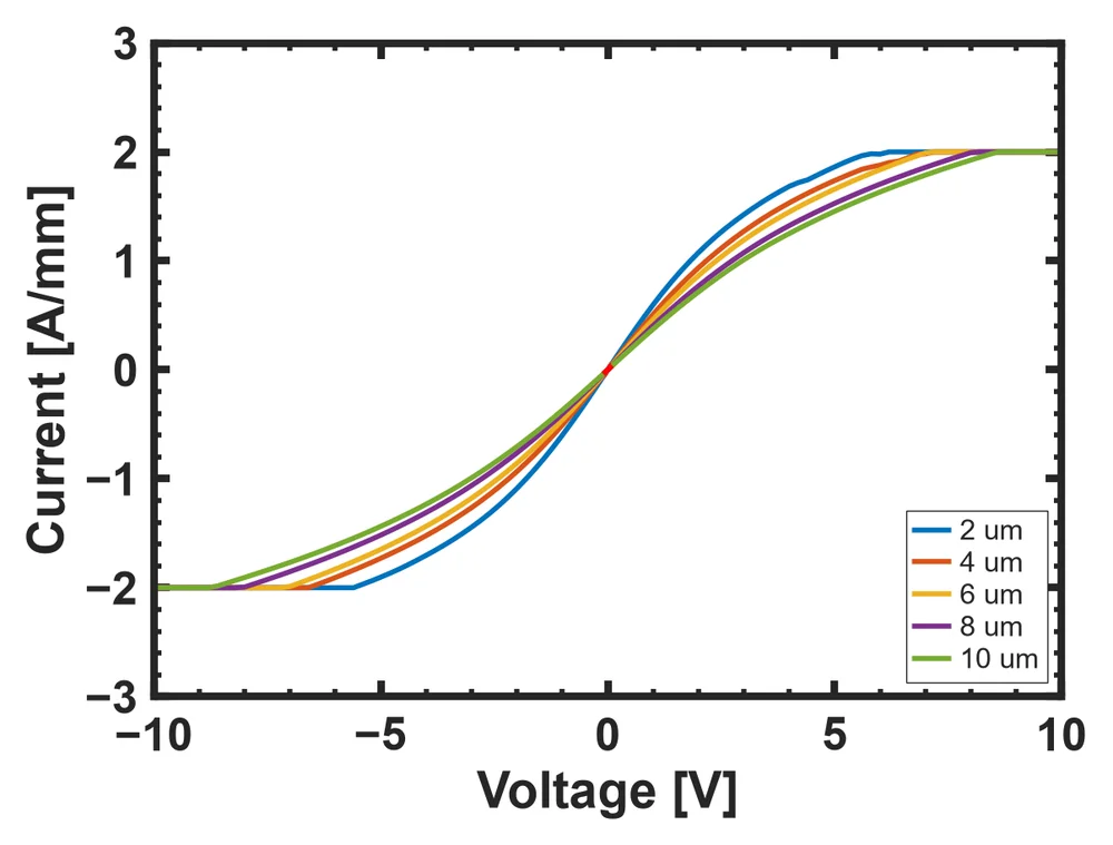
  • TLM · Rc 0.66–0.72 Ω·mm
  • Etch · +19% rate after a clean
Source-drain length against e-beam dose: 580 nm at 1100 down to 468 nm at 1400 microcoulombs per square centimetre, with a linear fit
Dose calibration
TLM current-voltage curves for gaps of 2 to 10 micrometres
TLM I–V, 2–10 µm

MIT · GabFab

GabFab, the fab tracker I built

Runs
Every sample, every step
TLM
Fits on upload
Assistant
Claude edits flows

Open GabFab ↗

GabFab run page: a checklist of process steps, each tracking four samples
GabFab TLM page: total resistance against gap length, with the fitDemo data

MIT · GabFab · Lab2Fab3D

The device, drawn from the traveler

  • Steps → cross sections
  • + GDS masks → the chip in 3D
Animated 3D view of a HEMT as each process step is appliedSynthetic masks
Animated cross section of a GaN HEMT building up step by step

Backup · IBM Research

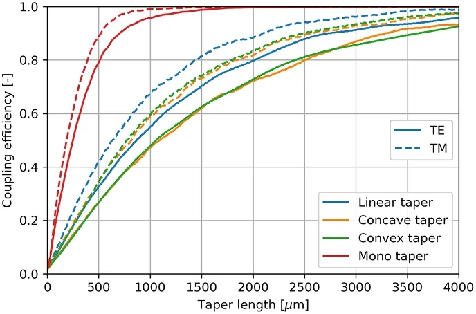
What sets a taper’s length

α(W) · dW/dz = ε  →  z(W) = (1/ε) ∫ α dW

  • α(W) = 1/C(W) peaks at phase match
  • Constant loss rate → the shape
  • Mono: 96% / 99% at 1 mm

Method and figures: J. Van Asch et al., J. Phys. Photonics 6, 045013 (2024), CC BY 4.0
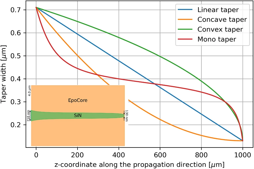
Taper width along a 1 mm SiN taper for linear, concave, convex and Mono shapes: the Mono taper narrows fast, then slowly around 0.35 to 0.45 micrometres, then fast again
Width along the taper
Coupling efficiency against taper length: the Mono taper passes 95 percent by about 1 mm, the others need about 3 to 4 mm
Coupling vs length

Backup · GabFab

How GabFab is built

App
Flask · SQLAlchemy
TLM
Plain-Python fits, with errors
Assistant
Claude · 42 tools
Cross sections
Steps → layer stack
3D
GDS reader · Three.js
InOut Traveler GDS masks I–V sweeps Notes, photos GabFabFlaskSQLAlchemy AssistantClaude · 42 tools Runs, trends TLM fits Cross sections 3D chip

Backup · Samsung

Dark-field inspection

  • Oblique laser; reflection misses the detector
  • Only scattered light → defects
  • Recipe: angle, polarization, aperture
Dark-field inspection detector oblique laser reflection misses it particle scattered light defect map
← fengfab.com 1 / 20